0x500 Accelerator
1. GPU
1.1. Computing
1.1.1. Streaming Multiprocessor (SM)
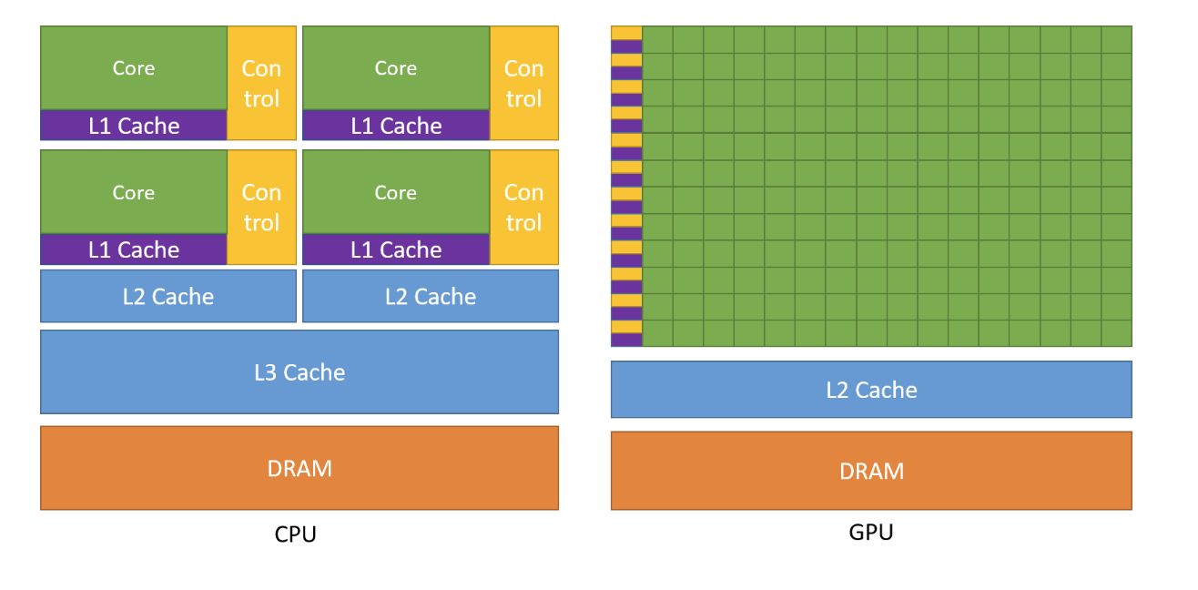
Conceptually, GPU have more cores but less cache and flow control compared with CPU
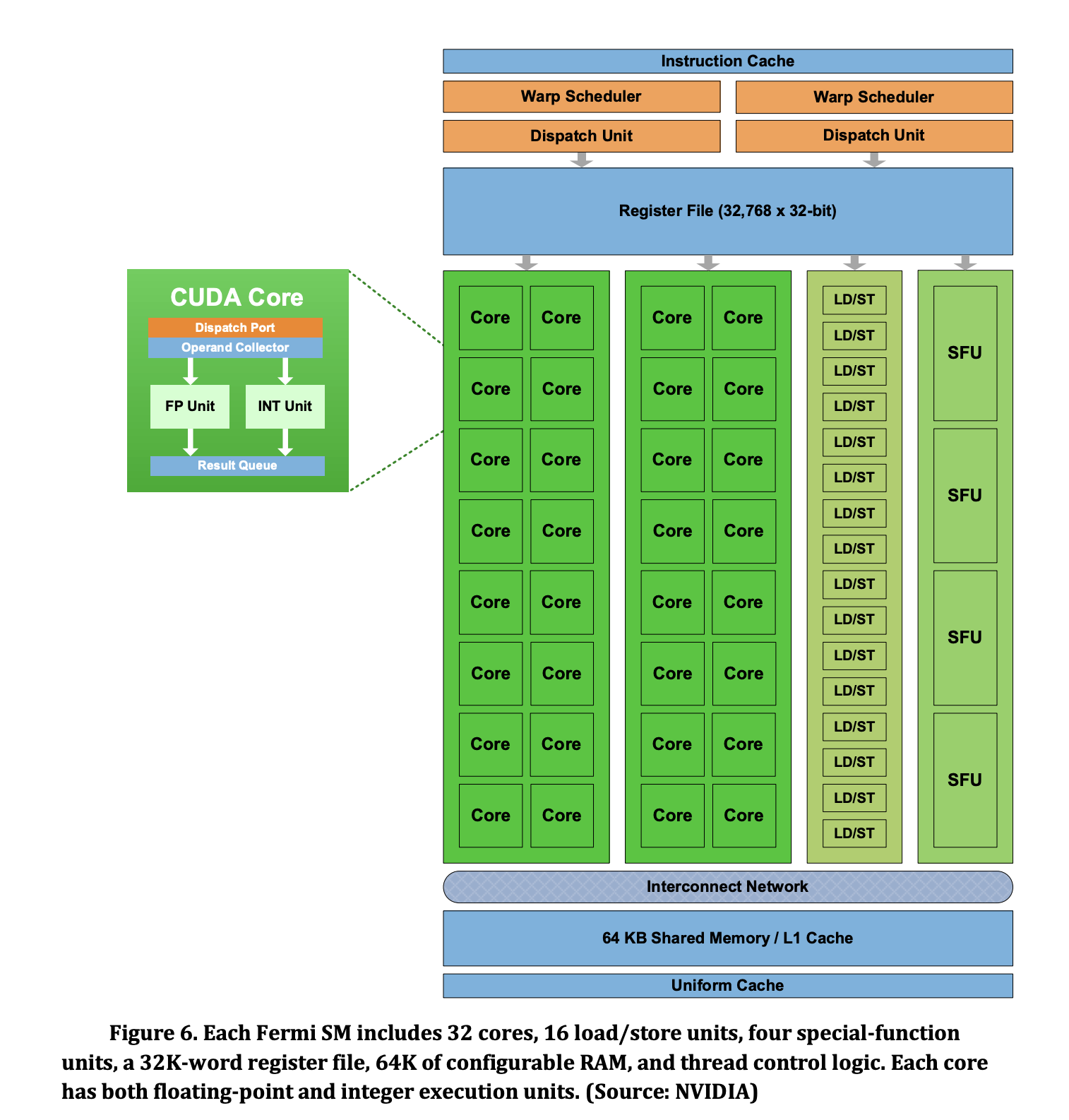
A Fermi's SM is illustrated as follows where
- each CUDA core can perform one single-precision fused multiply-add operation in each clock period
- large
- memory operations are hanlded by a set of 16 LD/ST (load/store) units in each SM by using two dimensional (x,y) values
- Special Function Units (SFU) is available to handle special operations such as sin, cos, exp
The recent generations are:
- Pascal
- Volta (Turing)
- Ampere
- Hopper
1.2. Memory
Memory Hierarchy is as follows:
Register
- private to threads
- has a large size to reduce context switching
- when register size is not enough, we use local memory, which is thread-private memory resides in global memory
Shared Memory
- on-chip memory SRAM
- shared by all threads within a block
L2 Cache
- caching instruction, data from global memory
- managed by hardware
Global Memory (Device memory)
- off-chip memory (DRAM) accessible from all threads
- persist across kernel launchs
Host Memory
- far far far away
1.2.1. Shared Memory
Striding through global memory is problematic. Shared memory latency is roughly 100x lower than uncached global memory latency
Bank Conflicts : shared memory is divided into equally sized memory modules (banks). If multiple threads requested the same memory bank, the accesses are serialized and efficienfcy drops.
1.2.2. Global Memory (HBM)
Global memory can be allocated using __device__ or cudaMalloc
__device__ int globalArray[256];

void foo()
{
    ...
    int *myDeviceMemory = 0;
    cudaError_t result = cudaMalloc(&myDeviceMemory, 256 * sizeof(int));
    ...
}
load/store instructions wrt global memory from a swap is usually coaleced into a few small transactions to minimize DRAM bandwidth. See this post for more details
1.2.3. Host Memory
Unified Virtual Addressing CUDA devices can share a unified address space with the host
1.3. Communication
To inspect communication links, use nvidia-smi nvlink -s
1.3.1. PCI
Typically, PCI is the protocol to communicate between CPU and GPU, PCI can be divided into lanes where bandwidth of a single lane (i.e. PCIe x1) depends on the generations:
- PCIe 4.0: 2GB
- PCIe 5.0: 4GB
- PCIe 6.0: 8GB
at best, PCIe x16 bandwidth is ~100GB/s
To transfer between Host/Device efficiently, we can
- use pinned host memory (i.e. swapping not allowed) before memcpy (this prevent CUDA driver from creating temporary pinned memory buffer), which can be done using
cudaMallocHost - batching small transfers into a single transfer.
- overlapping (see the following)
1.3.2. SXM
SXM is a high bandwidth socket to conenect GPU with higher performance than PCIs equivalents
1.3.3. NVLink
NVLink provides > 1TB/S bidirectional, direct GPU-to-GPU interconnection
NVLink Switch connect NVLinks to provide all-to-all GPU communication
1.3.4. InfiniBand
communications between interconnected nodes
1.3.5. GPUDirect
With CUDA-Aware MPI, we can MPI_Send and MPI_Recv from GPU directly to another GPU without going through host memory.
1.4. Programming Model
Thread: the computational elements is known as kernels (typically written in C), can be compiled into many threads executing the same program in parallel.
Block: Threads are grouped into threads blocks which will run on a single Streaming Multiprocessor (SM), so threads within the same block can cooperate and share memory. In each thread block, threads are divided into warps of threads (e.g. 32 threads), where warp is the fundamental unit of dispatch within a single SM, consisting dozens of CUDA cores (e.g. 128 cores)
Grid thread blocks are grouped into grids, each of which executes a unique kernel
1.4.1. ISA
PTX (Parallel Thread Execution) is a low-level parallel-thread execution virtual machine and instruction set architecture (ISA). PTX exposes the GPU as a parallel computing device. CUDA generate PTX instructions
SASS is the low-level assembly language that compiles to binary microcode, which executes natively on NVIDIA GPU hardware
1.4.2. Stream Management
CUDA stream is a sequence (queue) of device operations (e.g. kernel, data transfer).
Each device operation in CUDA run in a stream (default stream if not specified). It can be used to overlap data tranfer, host computing and device computing
1.5. Performance
See this doc
Arithmetic Intensity is formulated as the ratio between ops and byte.
Different DNN layers typically has idfferent arithmetic intensity. Some layer has low arithmetic intesities (e.g. ReLU activation, layer normalization)
2. TPU
2.1. Computing
TPU v4 peak flops: 275 TFLOPS
A few published papers mentioned TPU architecture: TPU v1, TPU v2, TPU v4
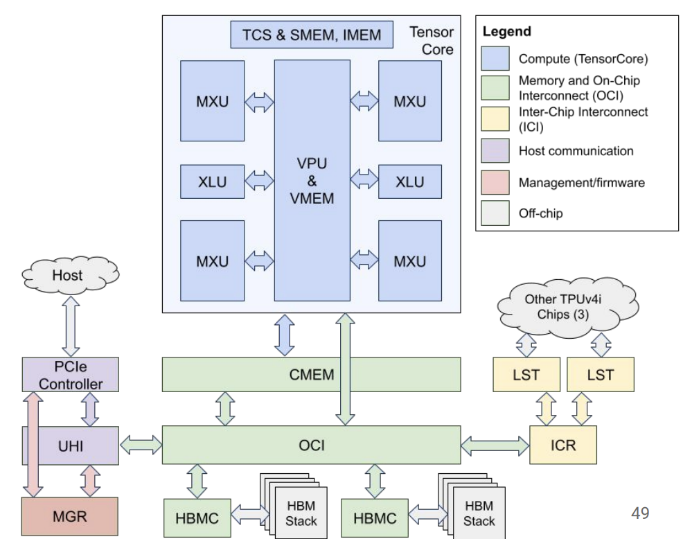
In general, from high-level to low-level hardware concepts:
- each pod is a contiguous set of TPUs grouped together over a specialized network
- each slice is a collection of chips all located inside the same TPU Pod connected by high-speed inter chip interconnects (ICI)
- each TPU chips have one or two TensorCores
- each TensorCore (i.e. TPU's core) has one or more matrix-multiply units (MXUs)
- each MXU is composed of 128 x 128 multiply-accumulators in a systolic array
2.1.1. TensorCore
Each TPU chip has 1 or 2 TensorCore depending on the generations
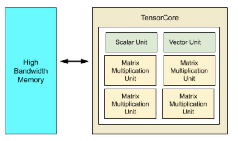
A single TensorCore has the following component:
scalar processor (SPU) used for control flow
vector processor (VPU) used for vector processing.
transpose-permute Unit: specialized for matrix transpose/permute
Matrix-multiply unit (MXU) is based on systolic array See this illustration to understand how matrix multiplication works in systolic array
- a single PE (processing element) is replaced with a regular array of PEs, where flow of data is carefully orchestrated orchestrated.
- array structure can be nonlinear and dimensional
Advantages:
- efficiently make use of limited memory bandwidth, balances computation to IO bandwidth
- specialized (computation need to fit PE organizaiton/functions)
Downside:
- not generally appliable
2.1.2. SparseCore
specialized for embedding lookup
2.2. Memory
TPU has no hardware-managed cache such as L1 and L2. all memory transfer is explicitly controlled by XLA
2.2.1. SMEM, VMEM
scalar memory, vector memory (organized in 2d 128x8), fast
2.2.2. CMEM
common memory, on-chip, small (128MB in gen4)
2.2.3. HBM
TPU v4: 32Gib, 120 GBps
slow memory
2.2.4. Infeed/Outfeed Queue
The TPU host streams data into an infeed queue. The TPU loads data from the infeed queue and stores them in HBM memory.
When the computation is completed, the TPU loads the results into the outfeed queue. The TPU host then reads the results from the outfeed queue and stores them in the host's memory.
2.3. Communication
Note that Gang-scheduling is essential in the case of TPUs, since they are single-threaded and only run non-preemptible kernels, so the system will deadlock if communicating computations are not enqueued in a consistent order
2.3.1. Host
TPU supports DMA to transfer
The TPU has two hardware queues: it loads data from the infeed queue and stores them in HBM memory. When the computation is completed, the TPU loads the results into the outfeed queue
2.3.2. ICI
TPU uses optical circuit switching instead of electrical packet switching as adopted by NVSwitch.
2.3.3. DCN
DCN (data-center network) connect between slices
3. CPU
3.1. Computing
3.1.1. AMX
Advanced Matrix Extensions (AMX) are extensions to x86 ISA, started from Sapphire Rapids microarchitecture for Xeon.
Its has using 2-dim registers and accelerator called matrix multiply unit (TMUL) performing tiled matrix multiplication.
4. Reference
- altera FPGA white paper
- What is a LUT
- A HN thread comparing FPGA with GPU
- Lecture on FPGA
- Operating Systems Three Easy Pieces