0x211 Semiconductor
1. Foundation
This documentary covers the early history of invention of transitor.
1.1. Pre-Transistor Era
See this video to understand how Vaccum tube works
Diode:
- Anode (P)
- Cathode (K)
Triode works as an amplifier, see this video
- Anode
- Grid
- Cathode
2. Transistor
Electrical conductivity of Semiconductor is between medal and insulator
Properties
- amplification
- switch
- energy transformation
Material - Group 14: Silicon, Germanium
Band
- Conduction band: electrons distributed here for medals
- Valence band: electrons distributed here for insulators
Doping
- N type: introducing redundent electron (n means negative, not the atom), examples are Phosphorus, Arsenic
- P type: electron hole (p means positive, not the atom), examples are Boron, Gallium
2.1. BJT
See this video
p-n junction
- forward bias: electron moves when voltage > 0.7V
- reverse bias: reverse voltage will widen energy of depletion layer
Bipolar Junction Transistor can be seen as two Diode connected reversely such as NPN or PNP, it is current controlled, mainly used for amplification
Invented by Shockley, Bardeen, Brattain at Bell Labs in 1947. (Nobel Prize awarded in 1956)
Component
- Base (i.e. switch)
- Emitter
- Collector
2.2. MOSFET
voltage controlled, mainly used for switch
Feature
- Little energy waste compared with Bipolar
- Building blocks of SRAM and CPU
- Scalable
Component
- Gate (i.e. switch)
- Source
- Drain
2.3. CMOS Logic
See this video to understand how P-MOS and N-MOS (i.e. complementary MOS) can be used to implement primitive logic gates. CMOS is better than N/P-MOS since it does not consume power (through resistor)
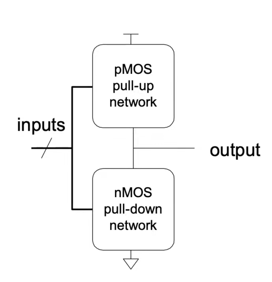
CMOS logic implementation is in the following style:
- one (out of the two) network should be ON and the other is off
- when nMOS network is in series, the pMOS network are in parallel
- when nMOS network is in parallel, pMOS network is in series
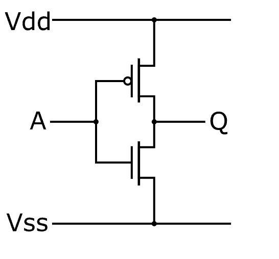
For example, inverter is implemented as follows
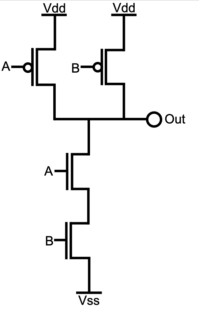
Nand is implemented as follows: