0x222 Computer Organization
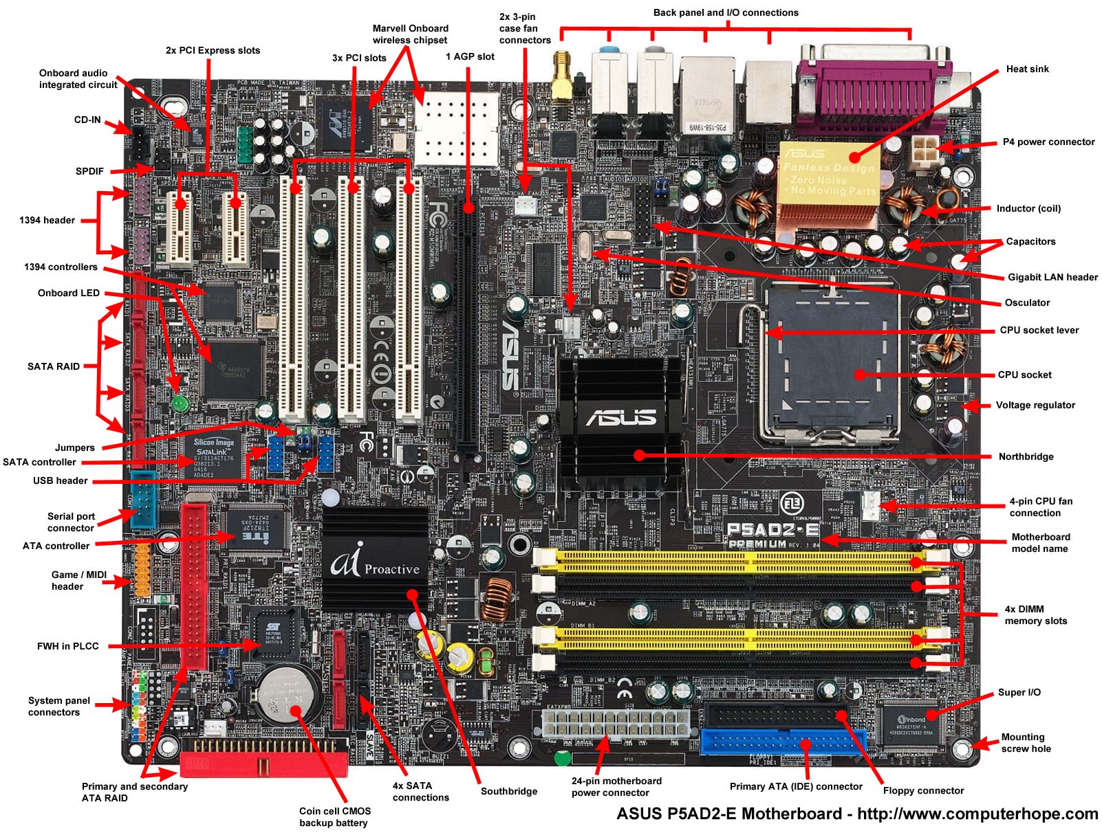
This page summarizes every peripheral and hardware interface/component connected to the motherboard except CPU. CPU related contents will go to the Processor page.
The traditional overview of the Hub architecture looks like this

a chipset is a set of electronic components in an integrated circuit known as a "Data Flow Management System" that manages the data flow between the processor, memory and peripherals. This video explains well
Chipset (Northbridge) a traditional chip, now went inside the CPU itself. It connects CPU and high-speed modules (DDR RAM and graphic card) Intel Management Engine: firmware is based on MINIX 3
Chipset (Southbridge) a traditional IO chip, now replaced by PCH (platform controller hub) in intel's chip, it connects northbridge with slow-speed modules To connect northbridge and southbridge, we can use DMI (direct media interface) which is Intel's proprietary link.
1. Bus
A bus is a shared communication link, which uses one set of wires to connect multiple subsystems. The advantages are versatility and low cost, the disadvantage is that it might create the communication bottleneck (e.g: through put)
Bus can be serial or parallel, serial is more commonly used today (e.g: s in USB, SATA, SCSI are all means serial)

1.1. Process-Memory Bus
usually short, high speed bus
1.2. IO Bus
lengthy, can have many types of devices connected to them, and can have a wide range in the data bandwidth.
PCI: faster, usually used for graphics and some other higher-performance IO peripheral bus: slower bus (e.g: SCSI, SATA, USB) connecting slow devices (e.g: keyboard, disks, mice)
1.2.1. AGP
1.2.2. PCI Express
bandwidth is determined by generation and length (adapted to lowest one). Here is a simple video tutorial.
Generation double bandwidth in each generation
- generation 1: 250GB/s
- generation 2: 500GB/s
- generation 3: 1GB/s
double bandwidth in each generation Length 1x, 2x, 4x, 8x, 16x 4x can fit into 8x but only half speed
1.2.3. USB
2. Device Interface
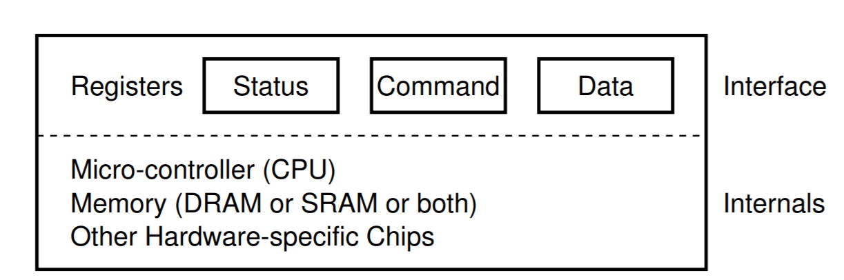
From the CPU's perspective, an I/O device appears as a set of special-purpose registers, of three general types:
- Status registers provide status information to the CPU about the I/O device. These registers are often read-only, i.e. the CPU can only read their bits, and cannot change them.
- control registers are used by the CPU to configure and control the device. Bits in these configuration registers may be write-only, so the CPU can alter them, but not read them back. Most bits in control registers can be both read and written.
- Data registers are used to read data from or send data to the I/O device.
The logic circuit that contains these registers is called the device controller, and the software that communicates with the controller is called a device driver.
There are mainly three types of protocols to transfer data between CPU, memory and IO devices.
2.1. programmed IO
Programmed IO (pooling) : CPU constantly monitor (polling) the status register of device, when free, write the command into the command register, and data into data register, waste of CPU when waiting long time.
It have two communication methods:
2.1.1. Memory Mapped IO
NOT TO BE CONFUSED WITH MMAP: mmap is to map a file to virtual address (OS in charge), this guy is to map phyiscal address to device register (CPU in charge)
Memory-mapped IO: use the same address space as main memory by map registering and ports. Access is done by normal load/store instructions. Common in RISC CPUs.
This web page have a good explanation about memory mapped IO.
2.1.2. Ported Mapped IO
Port-mapped IO: use the separate address space with dedicated instruction (e.g: x86 in/out)
2.2. Interrupt based IO
Interrupt based IO: issue the request and put the process to sleep, when device finish it, raise a hardware interrupt to wake out the process
2.3. DMA
DMA (direct memory access): A specific device that can orchestrate transfers between devices and main memory without much CPU usage.
Without DMA, when the CPU is using programmed input/output, it is typically fully occupied for the entire duration of the read or write operation, and is thus unavailable to perform other work. With DMA, the CPU first initiates the transfer, then it does other operations while the transfer is in progress, and it finally receives an interrupt from the DMA controller (DMAC) when the operation is done
The DMAC controller is a hardware device with the following registers (accessible from CPU):
- Address register: It contains the address to specify the desired location in memory.
- Word count register: It contains the number of words to be transferred.
- Control register: It specifies the transfer mode.
This page looks good
3. Memory
Memory are not only SRAM and DRAM, traditionally, we have the following technologies for the memory purpose. Watch this video from Crash Course.
- delay line memory (1944): store bit as sound pulse inside a long tube, which be can be detected with a microphone and then cycle back using transducer (speaker). This was used in EDVAC and EDSAC
- core memory (1951): induce a magnetic field into a tiny magnetic ring (core).
3.1. Architecture
3.1.1. Shared Address Space Model
Any processor can load and store from any address (shared address space)
3.1.2. UMA
symmetric multi-processor common one all memory access are post to the same bus
3.1.3. NUMA
each core has its local memory (but was also accessible form other cores)
3.2. SRAM
implemented with flipflop (4 or 6 transistors), used for cache
3.3. DRAM
1 bit is implemented with 1 capacitor + 1 transistor, used for main memory, watch this video for implementation.
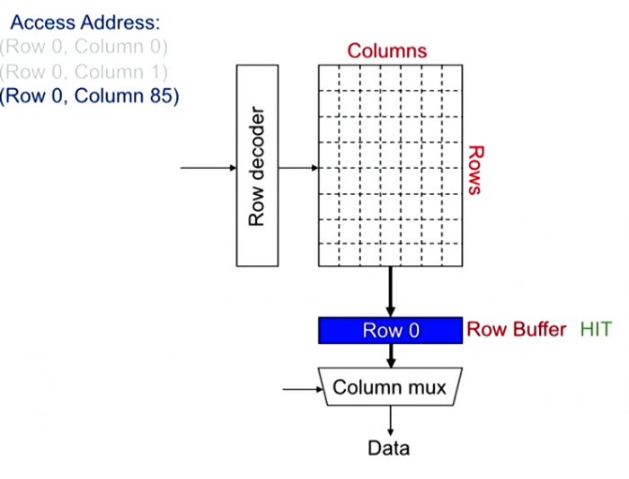
DRAM Bank Operation looks like following diagram. In the first step, row decoder selects one row, and send it to Row Buffer. Then column mux selects data. If the row buffer has already the correct row, then now need to fetch row. Typical Row size is 8KB, and request size is 64B.
DRAM Scheduling Policies
- row hit first: prioritize apps with high row buffer locality > apps with random access
- oldest first: prioritize memory-intensive applications
DRAM Latency
- reference: 100 ns
- 1mb sequential read: 0.25 ms
4. Storage Devices
4.1. Interface
4.1.1. SCSI
today only used in data center or as virtual interface. It was originall parallel, SCSI, now become Serial: SAS (Serial Attached SCSI).
SCSI command, bus, id
CPU->Host Bus Adaptor -> Target
Host Bus Adaptor translate PCI bus into SCSI bus
4.1.2. ATA
Originally PATA or IDE, now become Serial: SATA
This paper compares the SCSI and ATA in various perspectives.
4.2. Flash Memory
NAND flash memory and NOR flash memory
A good video on the structure of SSD
Structure of SSD
- The smallest element is the cell, depending on how many bits each cell can store (by different level), there are SLC (1 bit), MLC (2 bit), TLC (3bit) and QLC (4 bit) the SLC has the highest performance but the worst cost.
- Connecting those cell vertically gives a string (or vnand), consisting of around 100 cells.
- Connecting those cell horizontally gives a page, consisting of around 10k~100k cells, this is the minimum element for IO, usually 4KB.
- Page are organized into blocks by the order of 32~256 pages.
SSD Latency
- 4k random access: 0.15 ms
- 1mb sequential access: 1 ms
SSD Bandwidth
- SATA: 500M/sec
- PCI Express: > 1G/sec
4.3. Magenetic Disk
The address space scheme in magnetic disk is called Logical Block Addressing (LBA), it is linear addressing scheme starting from LBA 0. Block is the abstract concept of sector (might correspond to multiple sectors)
The address has been increased from IDE (22 bit), ATA-1 (28 bit) to ATA-6 (48 bit). The last one can address more than 100PB (2^48*512)
Geometry
- sector: 512 bytes, read/write is only atomic at this level
- track: each track is a concentric circle having many sectors
- surface: each surface is divided into multiple tracks
- platter: platter has 2 surface
We also have spindle, disk head and disk arm which moves around the platter. Watch this video to see to fast it is rotating/seeking!
IO Time:
- seek: move the head to the correct track (typically ~6 ms), it has many phases: acceleration, coasting and settling (this last guy is the most time consuming step)
- rotation: rotate the correct sector under head (this depends on the RPM, typically ~2 ms)
- transfer: read the data (this depends on the transfer rate, typically 100~200MB/s)
With those IO time, we can compute the following typical cases:
- disk seek: 10 ms
- 4kb read: 10 ms
- 1mb sequencial read: 20 ms
- 4kb random access: 0.3~0.6 MB/s
- sequential read: 100~200MB/s
Note that 4kb random access is a typical access pattern of DBMS
Note that IO can be checked with dd command in linux
OSTEP book homework chapter 38 has a good graphical animator to show how disk works
Scheduling:
The disk scheduler can manage which IO to be schedule next. The scheduler can be implemented by either OS or inside the device. Sometimes it is better to wait for a bit to issue the requests as a better request may arrive soon.
- Shortest seek time first: pick up the one minimize the seek time
- Elevator (SCAN, C-SCAN): move back and forth across the disk (to prevent starvation)
- Shortest positioning time first: consider seek and rotation time
4.4. RAID
RAID (Redundant Array of Inexpensive Disks) offer a number of advantages over a single disk:
- performance: speed up IO/times
- capacity: can store more data
- reliability: make the data vulnerable to the loss of a single disk
Suppose there are \(N\) disks, each with \(B\) blocks, a single disk has \(S\) MB/s for sequential workload and \(R\) MB/s for random workload
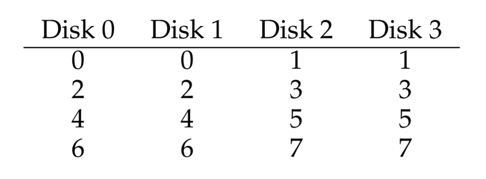
4.4.1. RAID 0 (Stripping)
Simply spread block across all disks. 1 disk failure will lead to data loss.
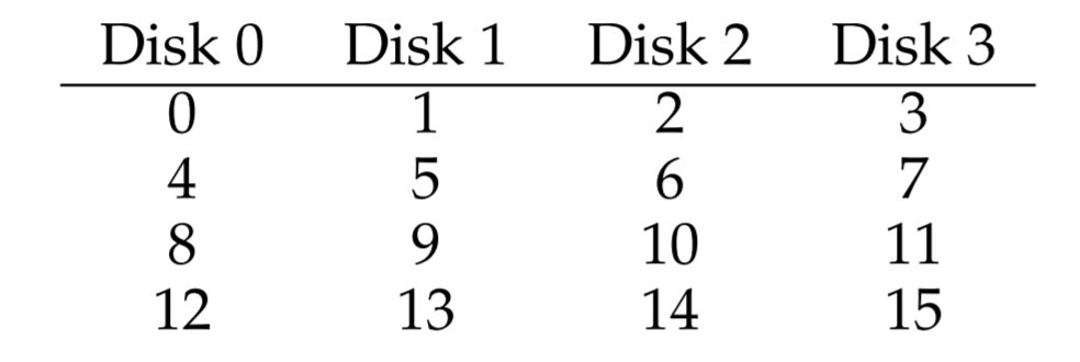
performance:
- Sequential Read: \(NS\)
- Sequantial Write: \(NS\)
- Random Read: \(NR\)
- Random Write: \(NR\)
capability: \(NB\) reliability: no reliability
RAID 1 (mirror)
Mirrroing can be combined with stripping as RAID-10 or RAID-01.
performance:
- Sequential Read: \(NS/2\)
- Sequential Write: \(NS/2\)
- Random Read: \(NR\)
- Random Write: \(NR/2\)
capability: \(NB/2\)
reliability: at least 1
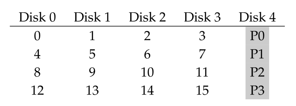
RAID 4 (parity)
Parity is computed by XORing the blocks in the same row. Write is typically a bottleneck as it requires the serializing IO to the parity disk
performance:
- Sequential Read: \((N-1)S\)
- Sequntial Write: \((N-1)S\)
- Random Read: \((N-1)R\)
- Random Write: \(R/2\)
capability: \((N-1)B\)
reliability: 1
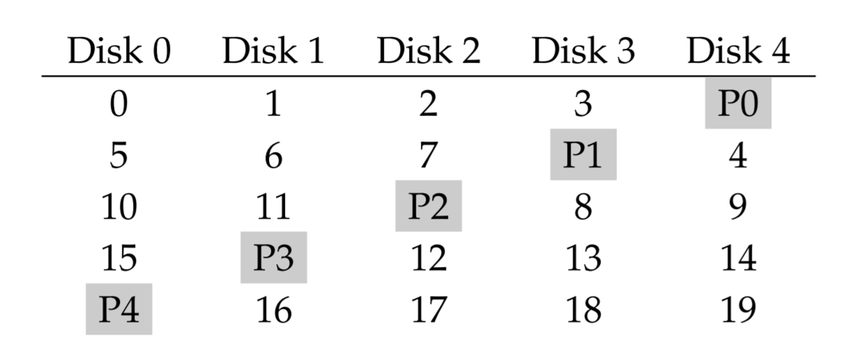
RAID 5 (rotating parity)
RAID 5 reduces the IO burden to the specific parity disk and spreading it across all disks
performance:
- Sequential Read: \((N-1)S\)
- Sequential Write: \((N-1)S\)
- Random Read: \(NR\)
- Random Write: \(NR/4\)
capability: \((N-1)B\)
reliability: 1
4.5. Tape Storage
5. Display
5.1. VGA
5.2. DVI
6. FPGA
FPGA provides faster hardware prototype and optimized hardware acceleration. Looks like modern FPGA is integrated with processors. But they are expensive, the price of Intel Stratix 10 looks like over 20k dollars.
6.1. Microarchitectures
System-on-Chip Products Altera (Intel): Arria 10 (used for NLU on bing) -> Stratix 10 Xilinx: Zynq Ultrascale+ LUT Look-Up Tables (LUT) is intended to implement arbitrary combinational logic.
implemented by MUX and SRAM. SRAM stores the configuration memory. The input is used to select the stored memory via MUX. Can simulate any truth table (e.g. : AND NOR ... ) Typically 6-LUTs Switches Switches can be configured to connect LUTs. It is something like bus
6.2. Synthesize
Language: Verilog or VHDL FGPA routing is a NP-hard problem (a disadvantage of FPGA) Reference: altera FPGA white paper What is a LUT A HN thread comparing FPGA with GPU Lecture on FPGA Operating Systems Three Easy Pieces
7. BIOS
BIOS is stored an ROM in the motherboard
7.1. CMOS
CMOS is a small memory to store the BIOS settings (it typically has a battery to make sure content does not disappear)
7.2. UEFI
Unified Extensible Firmwire Interface
- can handle larger disk than traditional BIOS
- support mouse
- has better GUI